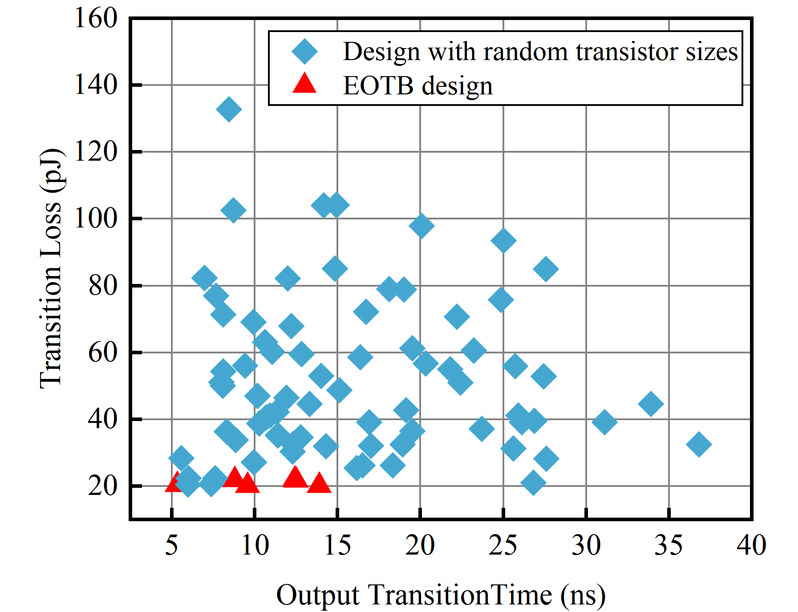
本文介绍了一种针对给定负载电容、输出过渡时间和源阻抗的渐变缓冲器的计算机辅助低功耗设计方法。进一步讨论了跨电压域渐变缓冲器,其中包括前级低电压域和后级高电压域,打破了传统设计中能量耗散与驱动能力之间的权衡。作为关键电路模块,提出了级移器的专用分析模型。在180纳米CMOS工艺中,对能量优化的渐变缓冲器设计在不同的源和负载条件下进行了验证。单VDD缓冲器模型与Spice模拟结果相比,平均不准确度为8.65%。跨电压渐变缓冲器可以进一步优化,显著降低能耗。该研究在能量高效的开关模式模拟应用中具有广泛的应用。
This paper introduces a computer-aided low-power design method for tapered buffers that address given load capacitances, output transition times, and source impedances. Cross-voltage-domain tapered buffers involving a low-voltage domain in the frontier stages and a high-voltage domain in the posterior stages are further discussed which breaks the trade-off between the energy dissipation and the driving capability in conventional designs. As an essential circuit block, a dedicated analytical model for the level-shifter is proposed. The energy-optimized tapered buffer design is verified for different source and load conditions in a 180-nm CMOS process. The single-??? buffer model achieves an average inaccuracy of 8.65% on the transition loss compared with Spice simulation results. Cross-voltage tapered buffers can be optimized to further remarkably reduce the energy consumption. The study finds wide applications in energy-efficient switching-mode analog applications.

